
RADIO が 2021年02月28日23時37分37秒 に編集
コメント無し
記事種類の変更
製作品
本文の変更
ATSとは自動列車停止装置のことで、実際の鉄道で使われているものです。これを、Nゲージ(1/150〜160の鉄道模型)で再現してみます。 といっても、あくまで自動で列車を停止させるだけで実際の鉄道で実装されている、パターン照査など高度なことはしていません。 また、この装置を使うことで、通常は同一線路上で1編成のみしか制御できないNゲージを、同時に複数制御することが可能になります。 @[youtube](https://youtu.be/hjAw2PbUgAY) **仕組み** レールを一定間隔ごとにギャップで区切り(絶縁)閉塞区間を設けます。ひとつの閉塞区間につき一編成のみ進入可能であり、閉塞区間に車両が進入した場合、その車両に対応するパワーパック(電源)を車両が進入した閉塞区間に接続する、というのが基本動作です。 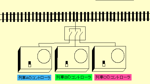 ==クリックするとアニメーションが見れます。== 制御はPICマイコンで行い、車両の位置はフォトカプラを使った電流検知回路で検出します。また、閉塞区間1つにつき、1つマイコンを使用し、隣接する閉塞空間に対応するマイコンとUARTで通信をしながら制御を行います。 **回路図** 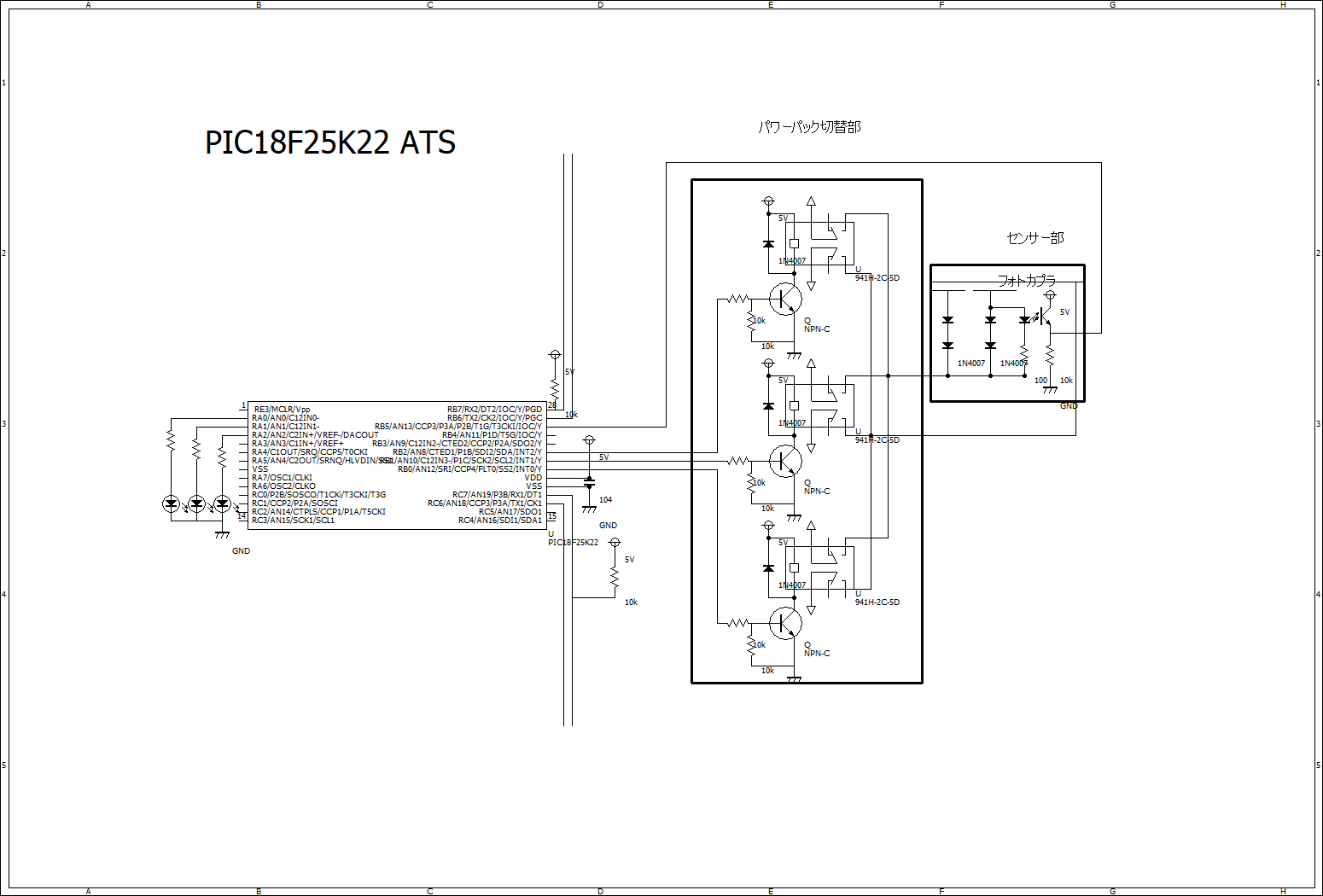 これが閉塞区間1つに必要な回路で、閉塞区間と同じ数だけ用意します。また、隣接する閉塞区間の回路との間で、UART1(JP1)と進行方向側隣接回路のUART2(JP2)、UART2(JP2)と進行方向逆側隣接回路のUART1(JP1)を接続します。 **ソースコード** ``` // PIC18F25K22 Configuration Bit Settings // 'C' source line config statements // CONFIG1H #pragma config FOSC = INTIO67 // Oscillator Selection bits (Internal oscillator block) #pragma config PLLCFG = OFF // 4X PLL Enable (Oscillator used directly) #pragma config PRICLKEN = ON // Primary clock enable bit (Primary clock enabled) #pragma config FCMEN = OFF // Fail-Safe Clock Monitor Enable bit (Fail-Safe Clock Monitor disabled) #pragma config IESO = OFF // Internal/External Oscillator Switchover bit (Oscillator Switchover mode disabled) // CONFIG2L #pragma config PWRTEN = ON // Power-up Timer Enable bit (Power up timer enabled) #pragma config BOREN = OFF // Brown-out Reset Enable bits (Brown-out Reset disabled in hardware and software) #pragma config BORV = 190 // Brown Out Reset Voltage bits (VBOR set to 1.90 V nominal) // CONFIG2H #pragma config WDTEN = OFF // Watchdog Timer Enable bits (Watch dog timer is always disabled. SWDTEN has no effect.) #pragma config WDTPS = 32768 // Watchdog Timer Postscale Select bits (1:32768) // CONFIG3H #pragma config CCP2MX = PORTC1 // CCP2 MUX bit (CCP2 input/output is multiplexed with RC1) #pragma config PBADEN = ON // PORTB A/D Enable bit (PORTB<5:0> pins are configured as analog input channels on Reset) #pragma config CCP3MX = PORTB5 // P3A/CCP3 Mux bit (P3A/CCP3 input/output is multiplexed with RB5) #pragma config HFOFST = OFF // HFINTOSC Fast Start-up (HFINTOSC output and ready status are delayed by the oscillator stable status) #pragma config T3CMX = PORTC0 // Timer3 Clock input mux bit (T3CKI is on RC0) #pragma config P2BMX = PORTB5 // ECCP2 B output mux bit (P2B is on RB5) #pragma config MCLRE = INTMCLR // MCLR Pin Enable bit (RE3 input pin enabled; MCLR disabled) // CONFIG4L #pragma config STVREN = ON // Stack Full/Underflow Reset Enable bit (Stack full/underflow will cause Reset) #pragma config LVP = ON // Single-Supply ICSP Enable bit (Single-Supply ICSP enabled if MCLRE is also 1) #pragma config XINST = OFF // Extended Instruction Set Enable bit (Instruction set extension and Indexed Addressing mode disabled (Legacy mode)) // CONFIG5L #pragma config CP0 = OFF // Code Protection Block 0 (Block 0 (000800-001FFFh) not code-protected) #pragma config CP1 = OFF // Code Protection Block 1 (Block 1 (002000-003FFFh) not code-protected) #pragma config CP2 = OFF // Code Protection Block 2 (Block 2 (004000-005FFFh) not code-protected) #pragma config CP3 = OFF // Code Protection Block 3 (Block 3 (006000-007FFFh) not code-protected) // CONFIG5H #pragma config CPB = OFF // Boot Block Code Protection bit (Boot block (000000-0007FFh) not code-protected) #pragma config CPD = OFF // Data EEPROM Code Protection bit (Data EEPROM not code-protected) // CONFIG6L #pragma config WRT0 = OFF // Write Protection Block 0 (Block 0 (000800-001FFFh) not write-protected) #pragma config WRT1 = OFF // Write Protection Block 1 (Block 1 (002000-003FFFh) not write-protected) #pragma config WRT2 = OFF // Write Protection Block 2 (Block 2 (004000-005FFFh) not write-protected) #pragma config WRT3 = OFF // Write Protection Block 3 (Block 3 (006000-007FFFh) not write-protected) // CONFIG6H #pragma config WRTC = OFF // Configuration Register Write Protection bit (Configuration registers (300000-3000FFh) not write-protected) #pragma config WRTB = OFF // Boot Block Write Protection bit (Boot Block (000000-0007FFh) not write-protected) #pragma config WRTD = OFF // Data EEPROM Write Protection bit (Data EEPROM not write-protected) // CONFIG7L #pragma config EBTR0 = OFF // Table Read Protection Block 0 (Block 0 (000800-001FFFh) not protected from table reads executed in other blocks) #pragma config EBTR1 = OFF // Table Read Protection Block 1 (Block 1 (002000-003FFFh) not protected from table reads executed in other blocks) #pragma config EBTR2 = OFF // Table Read Protection Block 2 (Block 2 (004000-005FFFh) not protected from table reads executed in other blocks) #pragma config EBTR3 = OFF // Table Read Protection Block 3 (Block 3 (006000-007FFFh) not protected from table reads executed in other blocks) // CONFIG7H #pragma config EBTRB = OFF // Boot Block Table Read Protection bit (Boot Block (000000-0007FFh) not protected from table reads executed in other blocks) // #pragma config statements should precede project file includes. // Use project enums instead of #define for ON and OFF. #include <xc.h> #define _XTAL_FREQ 16000000 int RX1data,RX2data; int a = 0,b = 0,c = 0; int sekkin_receive = 0; //接近受信を保存する int condition,forward_condition = 0; //状態 int henko_kyoka = 1; //0で禁止、1で許可する int data_count1,data_count2 = 0; int error1,error2 = 0; void PICsetup(){ OSCCON = 0b01110010; ANSELA = 0b00000000; // AN0-4 ???????????????I/O??? ANSELB = 0b00000000; // AN8-13???????????????I/O??? ANSELC = 0b00000000; // AN14-19???????????????I/O??? TRISA = 0b00000000; // RA0-RA7????????1??? 0??? TRISB = 0b10100000; // RB0-RB4 RB6??? RB5 RB7?????? TRISC = 0b10000000; // RC0-RC6??? RC7?????? LATA = 0b00000000; // ????????(??LOW???) LATB = 0b00000000; // ????????(??LOW???) LATC = 0b00000000; // ????????(??LOW???) } void USARTsetup(){ TXSTA1 = 0b00100100; RCSTA1 = 0b10010000; BAUDCON1 = 0b00001000; SPBRG1 = 0b10100000; SPBRGH1 = 0b00000001; CREN1 = 1; TXSTA2 = 0b00100100; RCSTA2 = 0b10010000; BAUDCON2 = 0b00001000; SPBRG1 = 0b10100000; SPBRGH1 = 0b00000001; CREN2 = 1; } void INTERRUPTsetup(){ RC1IF = 0; RC1IE = 1; RC2IF = 0; RC2IE = 1; PEIE = 1; GIE = 1; } void send(int num,int TXdata){ if(num==1){ while(TX1IF == 0); TXREG1 = TXdata; } if(num==2){ while(TX2IF == 0); TXREG2 = TXdata; } TXdata = 0; } void condition_henko(int i){ switch(i){ case 1: condition = 0; break; case 2: condition = 1; break; } } void __interrupt () receive(){ if( FERR1 || OERR1 ){ /* ????? */ CREN1 = 0; NOP(); CREN1 = 1; } if( FERR2 || OERR2 ){ CREN2 = 0; NOP(); CREN2 = 1; } if(RC1IF == 1){ RX1data = RCREG1; RC1IF = 0; a = 1; } if(RC2IF == 1){ RX2data = RCREG2; RC2IF = 0; b = 1; } } void kyuden(){ switch(sekkin_receive){ case 0: LATB0 = 0; LATB1 = 0; LATB2 = 0; __delay_ms(50); LATB0 = 1; break; case 1: LATB0 = 0; LATB1 = 0; LATB2 = 0; __delay_ms(50); LATB1 = 1; break; case 2: LATB0 = 0; LATB1 = 0; LATB2 = 0; __delay_ms(50); LATB2 = 1; break; } } int main(){ PICsetup(); USARTsetup(); INTERRUPTsetup(); while(1){ if(!(a == 0)){ if(a == 1){ sekkin_receive = RX1data; } if(condition == 2){ a = 2; }else{ condition = 2; henko_kyoka = 0; kyuden(); a = 0; } } if(b == 1){ forward_condition = RX2data; if(henko_kyoka == 1){ condition_henko(forward_condition); if(condition == 1){ send(1,1); } LATB0 = 0; LATB1 = 0; LATB2 = 0; c = 0; } b = 0; } if(PORTBbits.RB5 == 1){ if(!(c == 1)){ if(c == 0){ send(2,sekkin_receive); send(1,2); } if(forward_condition == 2){ LATB0 = 0; LATB1 = 0; LATB2 = 0; c = 2; }else{ henko_kyoka = 1; c = 1; } } } if(c == 2){ if(forward_condition == 2){ LATB0 = 0; LATB1 = 0; LATB2 = 0; c = 2; }else{ henko_kyoka = 1; c = 1; kyuden(); } } } } ``` **製作** 最初はユニバーサル基板で作ったのですが、配線ミスが多発し、3枚中1枚しか動きませんでした。いちいちミスを探すのも大変なので、プリント基板を使用することにしました。
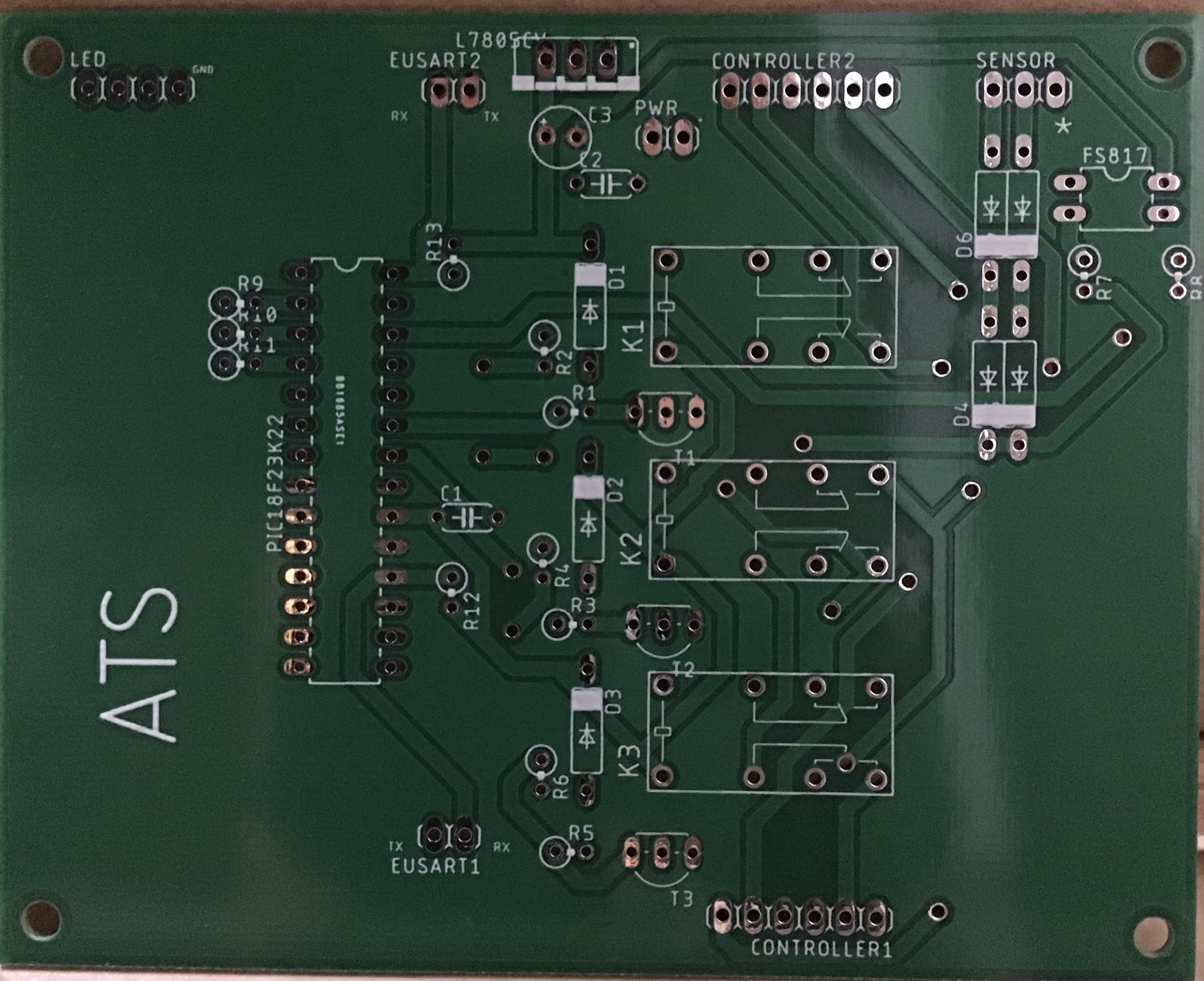 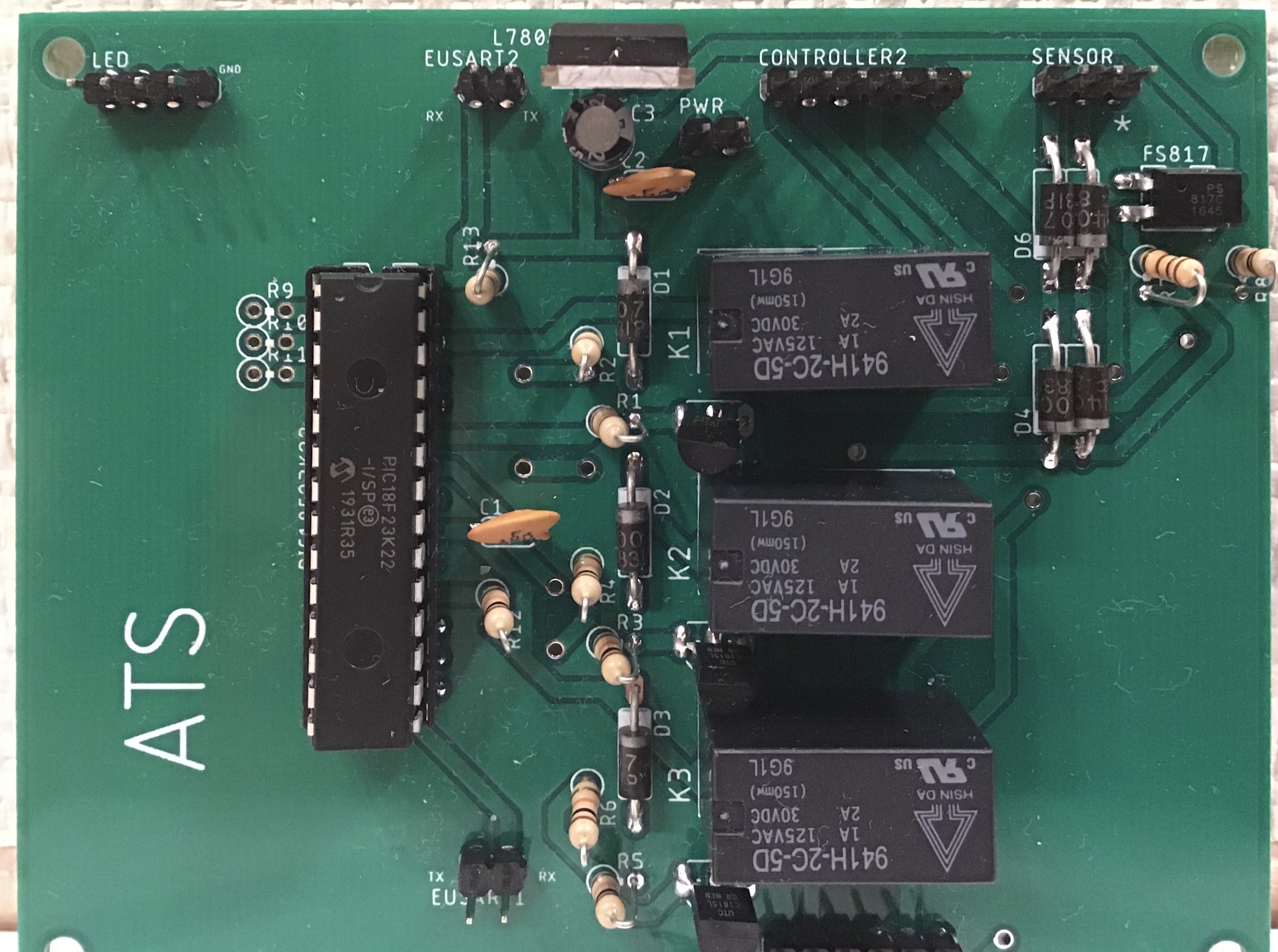
プリント基板はEAGLEで設計し、中国の格安基板製造業者PCBgogoに注文しました。