 セットアップや使用方法
  16
16Advanced 3D Packaging from Intel and AMD
In the era where Moore’s Law is approaching physical limits and transistor scaling is no longer the sole driver of semiconductor performance growth, 3D advanced packaging technology has become a core breakthrough for chipmakers to achieve heterogeneous integration, improve chip density and boost performance while controlling costs. As two giants in the global CPU and semiconductor industry, Intel and AMD have their own unique explorations and practical applications in 3D packaging technology. Intel’s Foveros-based Lakefield processor pioneered the mass production of 3D chiplet integration, while AMD’s 3D V-Cache (3D Vertical Cache) technology redefined the performance upgrade path of CPUs through innovative 3D stacking of cache chiplets. This article will delve into the technical details, structural design and industry significance of these two representative 3D packaging technologies from Intel and AMD.
Intel’s Lakefield Processor: The Pioneer of Mass-Produced 3D Chiplet Integration
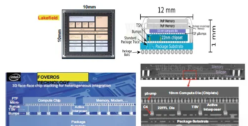
In July 2020, Intel officially launched the Lakefield mobile processor, a landmark product that marked the first large-scale mass production and commercial application of Intel’s proprietary Foveros 3D packaging technology. Breaking away from the traditional monolithic chip design, Lakefield adopted a revolutionary heterogeneous integration architecture, splitting the entire system-on-chip (SoC) functional modules into multiple independent chiplets and stacking them through advanced wafer-level integration processes – a design that not only optimized the chip’s physical size and power consumption but also set a precedent for the industrialization of 3D chiplet integration in the mobile computing field.
Core Technical Architecture of Lakefield
The core innovation of Lakefield lies in its chiplet disaggregation and 3D stacking design based on the Foveros technology platform. Intel split key functional modules of the mobile processor, including the central processing unit (CPU), graphics processing unit (GPU), LPDDR4 (Low Power Double Data Rate 4) memory controller and other peripherals, into separate chiplets with different process nodes and functional positioning. For example, the CPU module was divided into 1 large Golden Cove core and 4 small Tremont cores, each manufactured with the most suitable process for its functional characteristics to achieve the optimal balance of performance and power consumption.
These discrete chiplets are stacked on an active silicon interposer with Through-Silicon Vias (TSVs) through a face-to-face bonding process. This interposer, as the core interconnection "backbone" of the entire chip, is a large base chip manufactured with Intel’s 22nm ultra-low power (ULP) process, responsible for integrating and transmitting electrical signals between all chiplets to ensure efficient data interaction between different functional modules.
The multi-layer interconnection design of Lakefield is highly sophisticated and hierarchical, with different interconnection technologies adopted for different stacking layers to balance connection reliability, signal transmission speed and packaging density:
Chiplet to interposer interconnection: Micro-bumps (consisting of copper pillars and tin-silver solder caps) are used to realize the high-density electrical connection between each functional chiplet and the active silicon interposer, ensuring low-latency signal transmission between chiplets and the base interposer.
Interposer to package substrate interconnection: C4 (Controlled Collapse Chip Connection) bumps are adopted for the connection between the TSV silicon interposer and the ultra-simplified package substrate (only 4 coreless layers), which reduces the complexity of the substrate while ensuring stable power supply and signal output.
Package substrate to PCB interconnection: Traditional solder balls are used for the final connection with the printed circuit board (PCB), matching the mainstream industrial design of mobile devices and reducing the difficulty of downstream terminal application and production.
Compact Packaging Form and Product Features
Lakefield features an ultra-compact Package-on-Package (PoP) stacking form, with the entire package size only 12mm × 12mm × 1mm – a size that is far smaller than traditional mobile processors, perfectly adapting to the slim and light design needs of modern laptops, 2-in-1 convertibles and other mobile computing devices.
This PoP structure is divided into two upper and lower functional layers with a clear division of labor:
Lower layer: Integrates all core functional chiplets including CPU, GPU, memory controller and peripheral interfaces, the core carrier of Foveros 3D heterogeneous integration technology, which realizes the integration of computing, graphics and control functions in a tiny space.
Upper layer: Carries memory chips through the mature wire bonding technology, which is a complementary design for the PoP structure, further optimizing the integration density of the chip and avoiding the space waste caused by separate memory packaging.
Industry Significance of Lakefield
As Intel’s first mass-produced 3D packaging product, Lakefield has two pivotal industry significances: on the one hand, it is the world’s first mass-produced 3D chiplet integrated circuit product, verifying the technical feasibility and industrialization potential of 3D heterogeneous integration technology in large-scale production, and breaking the technical monopoly of traditional monolithic chip design; on the other hand, it is also the first mobile processor mass-produced through 3D IC integration technology, filling the gap of 3D packaging technology in the mobile computing field and providing a new design paradigm for the miniaturization and high performance of mobile chips.
Although Lakefield was later phased out due to market positioning and performance matching issues, its Foveros technology has become the core foundation of Intel’s subsequent advanced packaging layout, and has been continuously optimized and upgraded in products such as Intel’s Xeon server processors and Altera FPGAs, laying a solid technical foundation for Intel’s heterogeneous integration strategy.
AMD’s 3D V-Cache Technology: Redefining CPU Performance with 3D Stacked Cache
Following Intel’s exploration of 3D packaging, AMD launched the innovative 3D V-Cache (3D Vertical Cache) technology, which is a targeted 3D heterogeneous integration packaging solution for CPU performance improvement. Different from Intel’s Foveros technology that focuses on the disaggregation and stacking of multiple functional chiplets, AMD’s 3D V-Cache technology focuses on the 3D vertical stacking of CPU compute chiplets and SRAM cache chiplets, greatly increasing the CPU’s third-level cache (L3) capacity through advanced copper-copper hybrid bonding technology, thereby significantly reducing memory access latency and improving the parallel computing performance of the CPU – especially for high-performance computing (HPC), gaming and professional creative scenarios with high cache requirements. This technology has been widely applied in AMD’s Ryzen desktop CPUs and EPYC server CPUs, becoming a core competitive advantage of AMD’s high-end chips.
Tripartite Core Structure of 3D V-Cache
The 3D V-Cache packaging structure is a highly optimized three-layer chiplet integration design, consisting of three core components with clear positioning and complementary functions, and the structural balance and heat dissipation efficiency are fully considered in the design to ensure the stable operation of the 3D stacked chip:
Bottom Compute Chiplet: As the core computing unit of the entire structure, it is a CPU chiplet based on AMD’s "Zen 3" microarchitecture, manufactured with TSMC’s 7nm advanced process, with a chip area of 81 square millimeters. It integrates all the core computing resources such as CPU cores, instruction pipelines, and basic cache (L1/L2), and is the foundation of the entire chip’s computing power output.
Top SRAM Cache Chiplet: The core innovative component of 3D V-Cache technology, an extended L3 cache chiplet also manufactured with TSMC’s 7nm process, with a chip area of 41 square millimeters. This chiplet is exclusively responsible for providing ultra-large-capacity third-level cache, and through 3D vertical stacking, the L3 cache capacity of the CPU is increased by 3 times compared with the traditional monolithic design (for example, the AMD Ryzen 7 5800X3D has a 96MB L3 cache, which is three times that of the 5800X’s 32MB), effectively solving the bottleneck of memory access latency in high-load computing scenarios.
Structural Chiplet: A special functional chiplet designed for the 3D stacking structure, its core role is to maintain the structural balance of the entire 3D package and provide dedicated heat dissipation channels for the bottom compute chiplet. As the 3D stacked chiplet has a high integration density, the heat generated by the bottom compute chiplet is easily accumulated. The structural chiplet forms a reasonable heat dissipation path through its special structural design, which improves the overall heat dissipation efficiency of the chip and avoids performance throttling caused by overheating; at the same time, it compensates for the structural stress of the 3D stacking, reducing the risk of chip warpage and improving the reliability of the package.
Core Interconnection Technology: TSMC SoIC Copper-Copper Hybrid Bonding
The key to the realization of AMD’s 3D V-Cache technology lies in the adoption of TSMC’s System-on-Integrated-Chips (SoIC) copper-copper hybrid bonding technology, which is a revolutionary high-density interconnection technology far superior to traditional bump interconnection, and is also the core reason why 3D V-Cache can achieve ultra-low-latency cache access and high-reliability 3D stacking.
The interconnection design of the 3D V-Cache chiplet adopts a face-down stacking + back-to-front copper-copper bonding scheme: both the bottom compute chiplet with TSVs and the top SRAM cache chiplet are arranged in a face-down manner, and the interconnection between the two chiplets is realized through the back of the top chiplet and the front of the bottom chiplet via copper-copper hybrid bonding. The bonding interface of the entire chip is prepared by TSMC’s SoIC technology, with a copper-copper bonding pitch of only 9 microns – a far smaller pitch than traditional micro-bumps, which not only greatly improves the interconnection density between chiplets but also significantly reduces the signal transmission distance and latency between the compute chiplet and the cache chiplet, making the ultra-large-capacity 3D V-Cache truly play its role in improving CPU performance.
Industry Milestone of 3D V-Cache
AMD’s 3D V-Cache technology has created a new industry milestone: it is the world’s first computing unit product adopting copper-copper hybrid bonding technology for mass production, verifying the industrialization feasibility of TSMC’s SoIC high-density bonding technology in the field of high-performance computing chips, and pushing the 3D packaging technology from the traditional bump interconnection era to the more advanced copper-copper direct bonding era.
In terms of product performance, 3D V-Cache technology has achieved a qualitative leap in CPU cache capacity and performance. In gaming, content creation, cloud computing and other scenarios, the ultra-large-capacity L3 cache effectively reduces the CPU’s access to external memory, greatly improving the data processing speed and parallel computing efficiency of the chip. For example, AMD’s Ryzen 7 5800X3D has become a classic gaming CPU with its excellent cache performance and low latency, and the EPYC server CPU with 3D V-Cache has also achieved a significant improvement in cloud computing and HPC performance, helping AMD gain a larger market share in the high-end CPU market.
More importantly, AMD’s 3D V-Cache technology has opened up a new performance upgrade path for the semiconductor industry that is different from pure process scaling: under the background that the advanced process scaling is facing increasing technical difficulty and cost, through the innovative design of 3D packaging and heterogeneous integration, the chip performance can be significantly improved on the basis of the existing mature process, which provides a valuable reference for the subsequent development of the semiconductor industry and has become a typical case of the combination of advanced packaging technology and chip design innovation.
Core Differences and Industry Enlightenments of Intel and AMD’s 3D Packaging Technologies
Intel’s Foveros-based Lakefield and AMD’s 3D V-Cache represent two different technical routes of 3D advanced packaging in the industry at the initial stage of development: Intel focuses on full functional disaggregation and heterogeneous integration, splitting all functional modules of the chip into independent chiplets and stacking them through 3D packaging, pursuing the maximum flexibility of chip design and the optimal matching of process nodes; AMD focuses on targeted functional enhancement and dedicated stacking, aiming at the cache bottleneck of CPU, and realizing the performance upgrade through 3D stacking of cache chiplets, with a more targeted technical design and higher market application efficiency.
These two technical routes have brought important enlightenments to the global semiconductor industry: in the post-Moore’s Law era, advanced packaging technology has become an equally important core technology as transistor scaling, and heterogeneous integration and 3D stacking will be the mainstream development direction of the semiconductor industry in the future. Chipmakers no longer rely solely on shrinking the process node to improve chip performance, but can achieve diversified performance upgrades and product innovation through flexible packaging design, chiplet disaggregation and heterogeneous integration.
At the same time, the practice of Intel and AMD also shows that the development of 3D packaging technology cannot be separated from the close cooperation of the entire industrial chain: from the design of chiplets, the manufacturing of TSV interposers, to the high-density bonding technology and packaging testing, every link requires the joint efforts of chip design companies, foundries, packaging and testing enterprises and material suppliers. TSMC’s SoIC technology for AMD and Intel’s independent Foveros technology layout both prove that the mastery of core packaging technology has become a key factor for chipmakers to gain competitive advantages in the high-end market.
Conclusion
Intel’s Lakefield processor and AMD’s 3D V-Cache technology are two important milestones in the development of the global 3D advanced packaging industry. Lakefield pioneered the mass production of 3D chiplet heterogeneous integration, verifying the industrialization potential of 3D packaging technology and laying the foundation for the subsequent disaggregated design of chips; 3D V-Cache, on the other hand, through innovative copper-copper hybrid bonding and 3D cache stacking, redefined the performance upgrade path of CPUs and demonstrated the huge application value of advanced packaging technology in improving chip performance.
As the semiconductor industry continues to advance, Intel and AMD are also continuously optimizing and upgrading their 3D packaging technologies: Intel has extended Foveros technology to the server and data center fields, and launched more advanced packaging technologies such as EMIB (Embedded Multi-die Interconnect Bridge) and Foveros Omni; AMD has further upgraded 3D V-Cache technology to the Zen 4 and Zen 5 architectures, and expanded its application to the GPU and APU fields.
In the future, with the continuous innovation of high-density bonding, large-size interposer, panel-level packaging and other technologies, 3D advanced packaging will play a more important role in the fields of AI, high-performance computing, mobile electronics, automotive semiconductors and so on. The exploration and practice of Intel and AMD will continue to lead the technological development of the global semiconductor packaging industry, and push the entire industry toward a new era of heterogeneous integration and multi-chiplet collaboration.
投稿者の人気記事


-
LoveChip
さんが
前の土曜日の15:57
に
編集
をしました。
(メッセージ: 初版)
ログインしてコメントを投稿する